PCB /Dioxin treatment (detoxification)
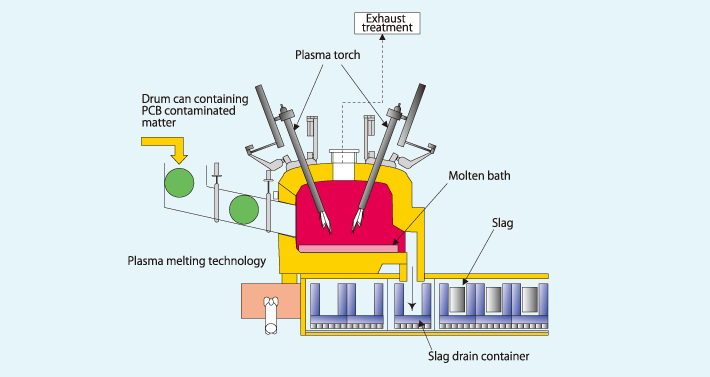
Plasma melting technology (co-developed with Nippon Steel Engineering Co. Ltd.) is a technology to treat in a batch PCB wastes with different forms and aspects, such as small electric devices including fluorescent light ballast, low voltage transformer and low voltage capacitor, sludge, waste cloth and carbonless paper, etc. The technology can destruct the PCB wastes by Synergetic effects of high-temperature plasma (over 15,000°C) and molten bath (over 1,400°C) generated by electric energy.
Features of the process
1. Various treatment objects
Various PCB wastes difficult to treat by normal cleaning and or heating separation can be destructed in a short time with enclosing them in a drum.
2. Improvement of work efficiency
As manual disassembly before treatment is not necessary, this process ensures high safety and work efficiency.
3. Exhaust safety
SOx, NOx, HCl and DXNs, etc. in exhaust gas are treated by multi-stage treatment equipment and finally go through the activated carbon.