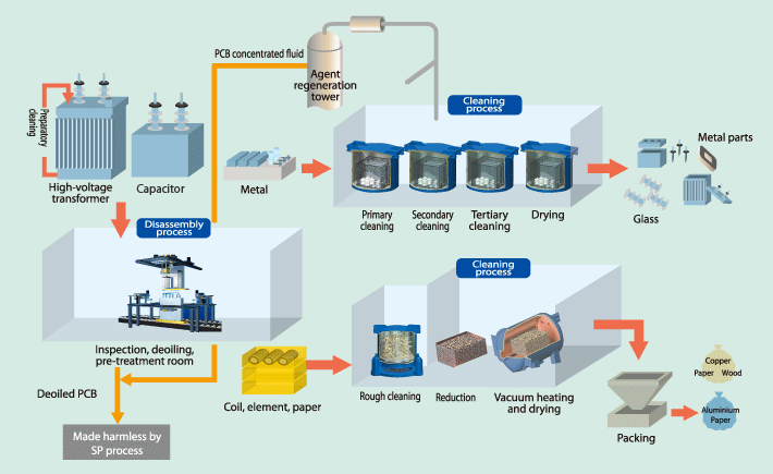
PCB wastes comtamination technology (SED process)
The SED process is a unique technology we developed to clean the contaminated equipment. It removes PCB from materials contaminated by PCB, i.e. transformer and capacitor, by cleaning with and vacuum heating separation hydrocarbon solvent. Removed PCB can be dissolved and detoxified by the SP process.
Features of the process
1. Decomposition with less PCB transpiration
Unnecessary transpiration of PCB is reduced by soak cleaning and shower cleaning while the contaminated devices are disassembled and separated into shapes suitable for cleaning.
2. Safety of cleaning solvent
Hydrocarbon solvent is used for cleaning of contaminated materials. In addition, cleaning solvent is recycled by distillation within the system.
3. Secure PCB removal
To ensure efficient and secure cleaning suitable for materials shapes, multiple cleaning methods such as ultrasonic cleaning, soak cleaning and mixing cleaning are combined.